|
|
Home Page
|
Futrfab – The Fab of Things
ABOUT FUTRFAB
|

What is a Futrfab and Who are the People Behind it?
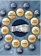
Futrfab, Inc. represents the culmination of almost a decade of research and visionary planning by a veteran fabrication Operations Manager for companies such as IBM and Philips Semiconductors. A Futrfab incorporates every aspect of the manufacturing process into one centralized location for…
|
The Fab of Things (FoT)
|
Today’s fabrication facilities simply don’t support small volume activities well.
With building costs in the billions of dollars, gross margin requirements—and the severe cost penalty of redesign—dictate what can and cannot be done. For example, in the semiconductor industry, Research and Development is often performed in shared facilities thousands of miles away from the designers…
|
THE FUTRFAB SOLUTION
|

Reopening Affordability for All Scales of Production
Large volume fabrication facilities simply don’t support small volume activities well. A Futrfab delivers superior work processes and dramatically decreased product cycle times rationalized to small volume needs and customers. It is an affordable, small volume manufacturing platform that will empower innovation…
|
|
Futrfab inc. – Enabling revolution through innovation.
|
|
See Our Videos
 Our founder, Dr. Fred Flitsch, discusses the revolutionary impact Our founder, Dr. Fred Flitsch, discusses the revolutionary impact
Futrfab’s patented processes will bring to technology manufacturing.
 The Futrfab environment incorporates every aspect of the manufacturing process into one centralized location. It will be the environment of choice for development of new types of components that incorporate or support electronics. The Futrfab environment incorporates every aspect of the manufacturing process into one centralized location. It will be the environment of choice for development of new types of components that incorporate or support electronics.
|
|